 CAM
CAM
Applying to the PCB manufacturing with designs for the productions by accuracy,speedy and stored specifications in computers.
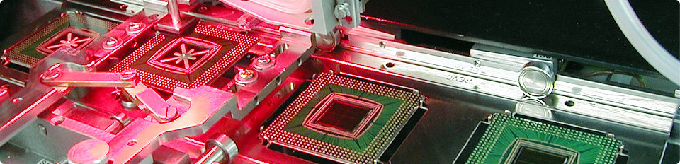
Drilling
This device is fitted with a 125,000rpm air spindle that allows for the drilling of 0.2mm holes, Drills for making holes are performed for plating holes to be electrical connecting between the top and bottom, and component's mounting on the boards
PTH
Electro-less copper plating: to metallize the wall of drilled holes, this hole matalization provides an electrical connection between the two sides of the board.
Pattern imaging
The circuit pattern is imaged on to each of the panels. The image defines the circuit for plating and the etching purposes. Negative circuit film is used for this purpose. Both sides of the panel are coated with a thin later of dry film photo resist.
Patterning plating
In this stage of the fabrication process, the thickness of copper tracks on the panels is increased by 20-30mm, over the copper tracks, tin-lead plating is done, which protect the conductive copper from oxidation there by preserving solder ability.
Etching
The dry film photo resist is stripped by a solvent, this bares the unwanted copper foil which is etched away to leave the plated circuit. Copper foil is etched by spraying the etched to both sides of the panel as it moves on a conveyor.
AOI
(AOI) equipment is used to inspect all inner layers before proceeding to the next step in production. This process identifies opens, shorts, and reduced traces. It is better to locate these problems early in the process, prior to lamination.
Multilayer Registration
Multilayer hole-to-pad registration is controlled utilizing Pluritech x-ray equipment. X-ray locates targets on the internal layers and creates tooling holes for the drilling according to the location of the internal pads.
Solder mask
solder mask is an epoxy barrier applied to one or more sides of the panels, it prevents solder bridges from forming during the wave soldering operation performed by the board user., it also reduces the ability of molten solder to adhere to the board’s surface..
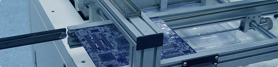
CNC routing
This is a process of dividing the single boards by automatic machine.
Testing
It focuses on checking each electrical point in order to make sure circuit is connected correctly.